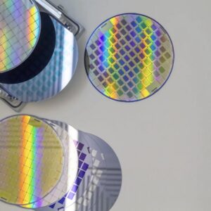
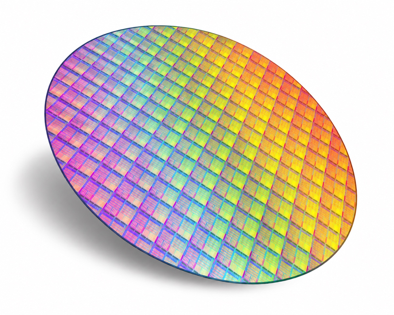
We supply new, unprocessed virgin silicon wafers — fresh single-crystal substrates grown and finished to your specification, never previously used, patterned or reclaimed. Every wafer is built to a written spec and shipped to SEMI standards for semiconductor R&D, MEMS, photonics, power devices and process development.
Crystal growth
- CZ (Czochralski) — the standard material for most device and general-purpose work.
- FZ (Float Zone) — high-purity, high-resistivity silicon for RF, power, radiation-detector and photonic applications.
Diameter & thickness
- Diameters of 2″ (50.8 mm), 3″, 4″ (100 mm), 5″/125 mm, 6″ (150 mm) and 8″ (200 mm), with 300 mm on request.
- Thickness to the SEMI standard for each diameter (for example ~280 µm at 100 mm, ~525 µm at 150 mm, ~725 µm at 200 mm) — plus thinned, thick and custom thicknesses to order.
- Primary/secondary flats or notch cut to SEMI orientation convention.
Electrical & crystallographic options
- Type & dopant: P-type (boron) and N-type (phosphorus, antimony, arsenic), plus intrinsic / high-resistivity material.
- Orientation: <100>, <111> and <110>.
- Resistivity: from <0.001 Ω·cm heavily doped to >20,000 Ω·cm intrinsic.
Surface finish
- SSP (single-side polished) and DSP (double-side polished).
- Thermal oxide and other film options on request.
All wafers ship new and virgin — no prior process — with full lot traceability. Share your diameter, type/dopant, orientation, resistivity, thickness and finish, and we’ll quote against it — request a quote.