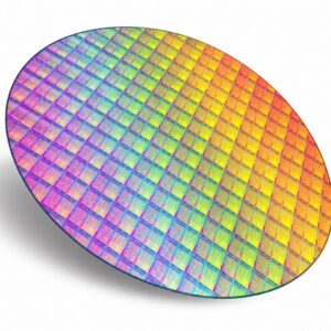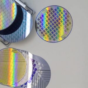
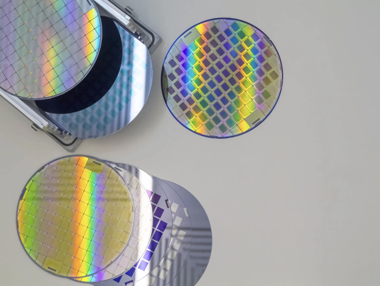
We supply reclaimed (reclaim) silicon wafers in 200 mm and 300 mm — used test, monitor and dummy wafers that have been stripped of their films, re-polished and particle-cleaned back to a usable surface. They are a cost-effective, sustainable substitute for prime silicon wherever a device-quality substrate is not required, and are supplied in the packaging format that suits your fab’s handling and shipping standard.
Sizes
- 200 mm (8″) and 300 mm (12″), to SEMI-standard thickness (typically ~725 µm at 200 mm and ~775 µm at 300 mm), with the correct flat or notch orientation.
- P-type or N-type base material; graded by particle count, TTV and number of reclaim cycles.
Reclaim process & grade
- Full film strip, chemical clean, re-polish (CMP / edge-polish as required) and final megasonic particle clean.
- Non-prime by definition (not for front-end device fabrication) — supplied as test / monitor / dummy grade against your particle and flatness limits.
Typical applications
- Tool qualification, chamber conditioning and equipment set-up.
- Particle and defect monitoring.
- Dummy / filler / handling wafers for batch tools.
- Process development and engineering runs.
Packaging options
- Coin roll — wafers stacked edge-to-edge in a protective roll for economical bulk quantities.
- FOSB (Front Opening Shipping Box) — the SEMI-standard sealed carrier for inter-fab shipping of 300 mm wafers.
- Cassette — open 25-slot H-bar cassette for 150/200 mm cleanroom transport and tool loading.
- JAR box — single-wafer jar / wafer box for individual, high-protection handling.
All reclaimed wafers are supplied with lot traceability. Tell us your size, base type, grade (particle / TTV limits), reclaim cycle and preferred packaging, and we’ll quote against it — request a quote.